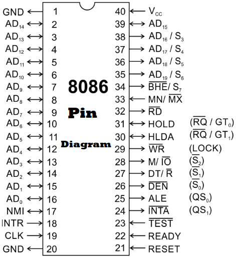
In this course, we will study the various Pin Diagram of 8086 Microprocessor that are present in the 8086 Microprocessor and its functioning. So let us start.
Pin Diagram of 8086 Microprocessor
There are 40 pins that are present in the 8086 microprocessor. There are 20 pins on each side of the IC.
Also learn, Pin Diagram of 8085 Microprocessor
What is the 8086 Microprocessor Pin Configuration?
AD0-AD15
These are the multiplexed bidirectional address or data bus. During the time T1, the lines carry a 16-bit address and in the remaining clock cycles, they carry data. AD0-AD7 carries the lower order byte of data and AD8-AD15 carries the higher-order byte of data.
Status signals
A16/S3, A17/S4, A18/S5, and A19/S6 are the multiplexed unidirectional address and status bus. During the time T1, they carry the higher-order 4-bit address and in the remaining clock, they carry status signals.
BHE/S7 is the fifth status signal. BHE stands for bus high enable. BHE is an active low signal. It is used to indicate the transfer of data over a higher-order data bus. It is multiplexed with the status pin S7.
RD
It is a read signal used for performing the read operation. It is an active low signal.
READY
Ready is an acknowledgement signal from the input/output devices. It is an active-high signal. Whenever we receive the ready signal it indicates that the device is ready to transfer the data.
RESET
It is a system reset. It is an active high signal. When the signal is high the system enters into the reset state and stops the current activity.
INTR
It is an interrupt request signal. It is an active high signal. It is level-triggered.
NMI
It is a non-maskable interrupt signal. It is an active high signal. It is edge-triggered.
TEST
It is used to test the status of math coprocessors of the 8087. The BUSY pin of 8087 is connected with this pin. If the signal is high the processor goes in the waiting state.
CLK
It provides the basic timing for processor operation. There are various frequencies like 5Hz, 8Hz, and 10Hz.
VCC AND VSS
VCC is the power supply signal and VSS is the ground signal.
MN/MX
The 8086 microprocessor works in two modes- minimum and maximum mode. If this pin is high the processor works in minimum mode and if it is low then it will work in maximum mode.
INTA
It is an interrupt acknowledgement signal. When the processor receives an interrupt signal it acknowledges the interrupt by generating this signal. It is an active low signal.
ALE
It is an address latch enable signal. It indicates that the valid address is available on the bus. It is an active high signal.
DEN
It is a data enable signal. This signal is used to enable the 8286 transceivers. The transceiver is used to separate the data from the address/data bus. It is an active low signal.
DT/R
This is a data transmit/receive signal. This signal decides in which direction data flows through the receiver. When the signal is high the data is transmitted out and when it is low the data is received in.
M/IO
This signal is issued by the microprocessor to distinguish memory access from the i/o access. When the signal is high the memory is accessed and when it is low the i/o devices are accessed.
Also learn, Block Diagram of 8085 Microprocessor
WR
It is a write signal. It is used to write data in memory or output devices. It is an active low signal.
HLDA
It is a hold acknowledgement signal. It is issued after receiving the hold signal. It is an active high signal.
HOLD
When the DMA controller needs to use the address/data bus, it sends a request to the CPU through this pin. It is an active high signal.
