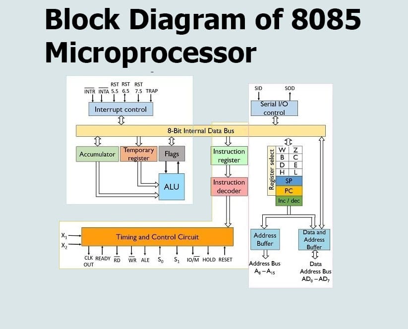
In this course, we will study what is 8085 Microprocessor & the Block Diagram of 8085 Microprocessor, and its functional units. So let us start.
What is 8085 Microprocessor?
The 8085 microprocessor is an 8-bit microprocessor. It consists of a 40-pin I.C. package and is fabricated on a single LSI chip. The Intel 8085 only uses a single +5V DC supply for its operation. The clock speed of the microprocessor is about 3MHz and the clock cycle is 320 ns. The time for the clock cycle of Intel 8085AH-2, the version is 200 ns. It consists of 80 basic instructions and 256 opcodes. There are three main sections in 8085 microprocessors: arithmetic and logic units, a timing and control unit, and a set of registers.
The Block Diagram of 8085 Microprocessor
What are the functional units in an 8085 Microprocessor?
8085 Microprocessor Functional Units are –
Accumulator in 8085 Microprocessor
This is the first unit in the Block Diagram of 8085 Microprocessor. It is an 8-bit register that is used for performing various operations like arithmetic, logical, I/O & LOAD/STORE operations. It is connected to the internal ALU and data bus.
Arithmetic and logic unit in 8085 Microprocessor
This is the second unit in the Block Diagram of 8085 Microprocessor. As the name itself suggests, it is used to perform arithmetic and logical operations on the data like Addition, Subtraction, AND, OR, etc. on 8-bit data.
General-purpose register in 8085 Microprocessor
This is the third unit in the Block Diagram of 8085 Microprocessor. There are 6 general-purpose registers that are present in the 8085 processor, i.e. B, C, D, E, H & L. Each register can hold 8-bit data.
These registers can operate to hold 16-bit data in pairs and their pairing combinations are like B-C, D-E, and H-L.
Program counter in 8085 Microprocessor
This is the 4th unit in the Block Diagram of 8085 Microprocessor. It is a 16-bit register that is used for storing the memory address location of the next instruction to be executed. The microprocessor increments the program whenever an instruction is being executed so that the program counterpoints to the memory address of the next instruction that is going to be executed.
Stack Pointer in 8085 Microprocessor
This is the 5th unit in the Block Diagram of 8085 Microprocessor. It is also a 16-bit register that acts like a stack, which is always incremented/decreased by 2 during push and pop operations.
Temporary register in 8085 Microprocessor
This is the 6th unit in the Block Diagram of 8085 Microprocessor. It is an 8-bit register, that is used to hold the temporary data of operations performed like arithmetic and logical operations.
Flag Register in 8085 Microprocessor
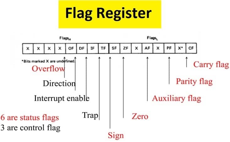
This is the 7th unit in the Block Diagram of 8085 Microprocessor. It is an 8-bit register consisting of five 1-bit flip-flops that can hold either 0 or 1 depending upon the result that is stored in the accumulator.
These are the set of 5 flip-flops −
- Sign (S)
- Zero (Z)
- Auxiliary Carry (AC)
- Parity (P)
- Carry (C)
Sign Flag (S)
After the completion of any operation, if the MSB (B(7)) of the result is 1, this indicates that the number generated is negative and the signal flag is set, i.e. 1. In case if the MSB is 0, it indicates that the number generated is positive and the sign flag becomes reset i.e. 0.
from 00H to 7F, sign flag is 0
from 80H to FF, sign flag is 1
1- MSB is 1 (negative)
0- MSB is 0 (positive)
Zero Flag (Z)
After any arithmetic or logical operation, if the result is 0 (00)H, the zero flags become set i.e. 1, otherwise, it becomes reset i.e. 0.
00H zero flags are 1.
from 01H to FFH zero flag is 0
1- zero result
0- the non-zero result
Auxiliary Carry Flag (AC)
This flag is used in the BCD number system (0,1,2,3,4,5,6,7,8,9). After any arithmetic or logical operation if D(3) generates any carry and passes it on to B(4) this flag becomes set i.e. 1, otherwise, it becomes reset i.e. 0. This is the only flag register that can not be accessed by the programmer.
1-carry out from bit 3 on an addition or borrow into bit 3 on subtraction
0-otherwise
Parity Flag (P)
After any arithmetic or logical operation if the result generated has even parity that means it has an even number of 1 bit, the parity register becomes set i.e. 1, otherwise it becomes reset i.e. 0.
1-accumulator has an even number of 1 bit
0-accumulator has odd parity
Carry Flag (CY)
It is generated in the case when performing n bit operations and the result comes out to be more than n bits, then this flag becomes set i.e. 1, otherwise, it becomes reset i.e. 0.
During subtraction (X-Y), if X>Y it becomes reset and if (X < Y) it becomes set.
The carry flag is also called the borrow flag.
1-carry out from MSB bit on the addition or borrow into MSB bit on subtraction.
0-no carry out or borrow into MSB bit.
Instruction register and decoder in 8085 Microprocessor
This is the 8th unit in the Block Diagram of 8085 Microprocessor. The instruction register and decoder are 8-bit registers. At the very moment when an instruction is fetched from memory, it is stored in the Instruction register. The instruction decoder is responsible for decoding the information present in the Instruction register.
Timing and control unit in 8085 Microprocessor
This is the 9th unit in the Block Diagram of 8085 Microprocessor. It provides timing and control signals for the microprocessor to operate. These are the timing and control signals, which control various external and internal circuits.
Control Signals: READY, RD’, WR’, ALE
Status Signals: S0, S1, IO/M’
DMA Signals: HOLD, HLDA
RESET Signals: RESET IN, RESET OUT
Interrupt Control in 8085 Microprocessor
This is the 10th unit in the Block Diagram of 8085 Microprocessor. The interrupt control controls the interrupts during a process. During the execution of the main program, whenever an interrupt occurs, the control is shifted from the main program to process the incoming request. After the completion of the request, the control again goes back to the main program.
There are 5 interrupt signals in 8085 microprocessors: INTR, RST 7.5, RST 6.5, RST 5.5, and TRAP.
Serial Input/Output Control
This is the 11th unit in the Block Diagram of 8085 Microprocessor. It is responsible for controlling the serial data communication by using two instructions: SID (Serial input data) and SOD (Serial output data).
Address buffer and address-data buffer
This is the 12th unit in the Block Diagram of 8085 Microprocessor. The content that is stored in the stack pointer and program counter is loaded into the address buffer and address-data buffer for communicating with the CPU. These buses are connected to the memory and input/output chips; the CPU can exchange the desired data with the memory and input/output chips.
Address bus and data bus
This is the 13th unit in the Block Diagram of 8085 Microprocessor. The data bus only carries the data that is to be stored. It is bidirectional, whereas the address bus carries the location to where it should be stored and it is unidirectional. It is also used for transferring data & Address I/O devices.

