In this course, we will study what is Instruction Cycle in Microprocessor and the Timing Diagram in Microprocessor & machine cycles in Microprocessor. So let us start.
Instruction Cycle in Microprocessor
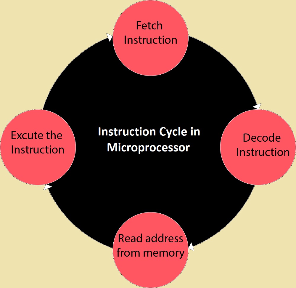
The time required for the completion or execution of one instruction is known as the Instruction Cycle in Microprocessor. The instruction cycle consists of a –
- Fetch Instruction Cycle in Microprocessor
- Decoding Instruction Cycle in Microprocessor
- Reading effective address Instruction Cycle in Microprocessor
- Execution Instruction Cycle in Microprocessor
Fetch Instruction Cycle in Microprocessor
The next instruction is fetched by the address stored in the program counter (PC) and then stored in the instruction register.
Decode Instruction Cycle in Microprocessor
The decoder interprets the encoded instruction from the instruction register.
Reading effective address Instruction Cycle in Microprocessor
The address given in the instruction is read from the main memory and the required data is fetched. It depends on the direct addressing mode or the indirect addressing mode.
Execution Instruction Cycle in Microprocessor
It consists of the memory read (MR), memory write (MW), input-output read (IOR) and input-output write (IOW).
Machine Cycles in Microprocessor
- The time which is required for accessing the memory or input/output devices is called a machine cycle in a Microprocessor.
- One to four machine cycles are used.
- For example, memory reading, memory writing, opcode fetches, etc.
- One machine cycle is equal to 12 clocks.
- One machine cycle consists of 6 states.
What are the T states in Microprocessor?
- It is one subdivision of the operation performed in one clock period.
- It is part of the machine cycle.
- One clock period is equal to one t state.
- One machine cycle is equal to 12 t states.
Timing Diagram in Microprocessor
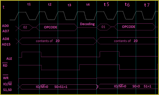
The timing diagram in Microprocessor is a graphical representation. It is used for the representation of the execution time taken by each instruction in a graphical format. The t states represent the timing diagrams.
- CLOCK – It is the clock pulse provided to the user.
- AD0-AD7 – These are used to carry data and addresses. It is the lower address bus. The decision of when it will carry an address and when it will carry data is made by ALE.
- A8-A15– It is used to carry the address bits.
- ALE – It provides the signal for multiplexed addresses and data buses. If the signal is high or 1, a multiplexed address and data bus will be used as an address bus. To fetch a lower bit of address, the signal is 1 so that the multiplexed bus can act as an address bus. If the signal is low or 0, the multiplexed bus will be used as the data bus. When a lower bit of address is fetched then it will act as a data bus as the signal is low.
- RD (low active) – If the signal is high or 1, no data is read by the microprocessor. If the signal is low or 0, data is read by the microprocessor.
- WR (low active) – If the signal is high or 1, no data is written by the microprocessor. If the signal is low or 0, data is written by the microprocessor.
- IO/M (low active) and S1, S0 – If the signal is high or 1, the operation is performed on the input-output. If the signal is low or 0, the operation is performed on memory.
Thanks for giving your time to us for learning Instruction Cycle in Microprocessor and Timing Diagram in Microprocessor. I hope you like this tutorial.

