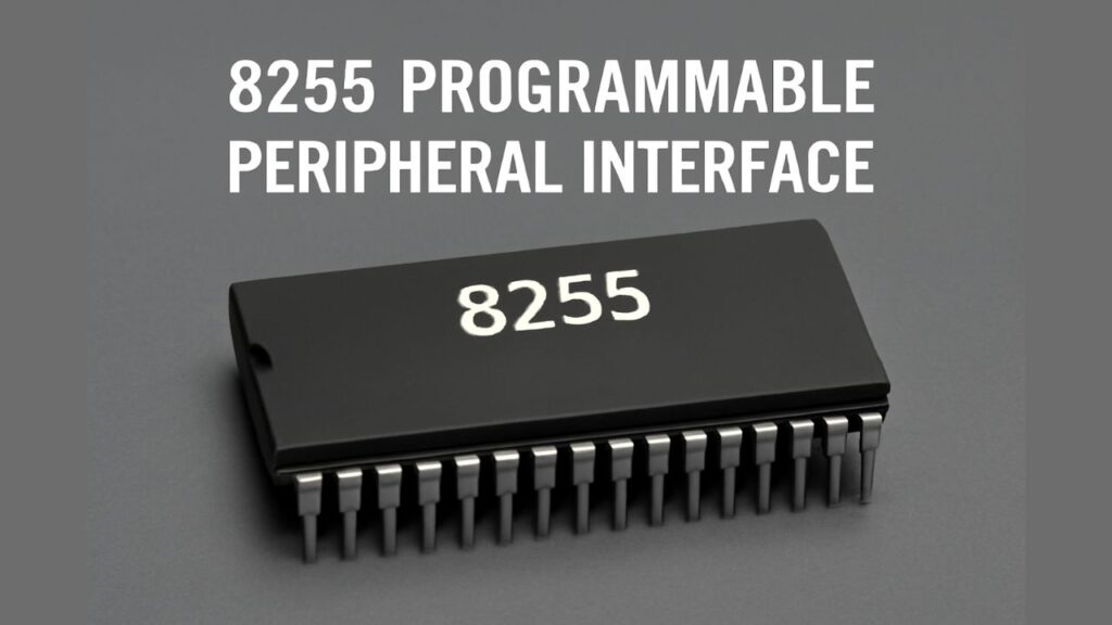
This article will talk about the 8255 programmable peripheral interface. In reality, there is no direct way to link I/O devices to the processor’s data bus. Consequently, it must be replaced with an 8255 microprocessor or another device that has I/O ports for connecting I/O devices. This processor belongs to Intel’s MCS-85 family and is compatible with both the 8086 and 8085 microprocessors.
Also learn: Microprocessor vs Microcontroller
The 8255 programmable peripheral interface, 8255, is a peripheral interface device that can be programmed to make fundamental connections between machines and microprocessors. It is an accessory for a computer that has been configured to function as an interface. The 8255 PPI serves as a bridge between microprocessors and I/O devices. An overview of the 8255 programmable peripheral interface and its functional applications is covered in this article.
8255 Programmable Peripheral Interface
The PPI 8255 programmable peripheral interface is a general-purpose programmable I/O device designed to link the CPU to external devices like as DACs, ADCs, and keyboards. By the specified condition, we can program it. Almost any microprocessor can use it. PORT A, PORT B, and PORT C are its three 8-bit bidirectional I/O ports. Various ports can be designated as input or output functions.
In 8255 programmable peripheral interface, It runs on a +5V regulated power source and has 40 pins. Port C can function in either mode 0 of the 8255 input-output mode or BSR (bit set rest) mode. Port C lower and port C upper are the two 4-bit ports into which it is further separated. In the input-output mode, port B can operate in either mode 0 or mode 1. Port A can function in either mode 0 or mode 1 while in the input-output mode. Control group A and control group B are its two control groups. Ports A and C upper make comprise control group A. Port B and port C lower make up control group B. We can choose different ports in various modes as input-output functions, or BSRs, based on the values of CSs, A1, and A0. Writing an appropriate word in the control register (control words D0-D7) accomplishes this.
| CS’ | A1 | A0 | Selection | Address |
|---|---|---|---|---|
| 0 | 0 | 0 | PORT A | 80 H |
| 0 | 0 | 1 | PORT B | 81 H |
| 0 | 1 | 0 | PORT C | 82 H |
| 0 | 1 | 1 | Control Register | 83 H |
| 1 | X | X | No Selection | X |
8255 programmable peripheral interface – Pin Diagram
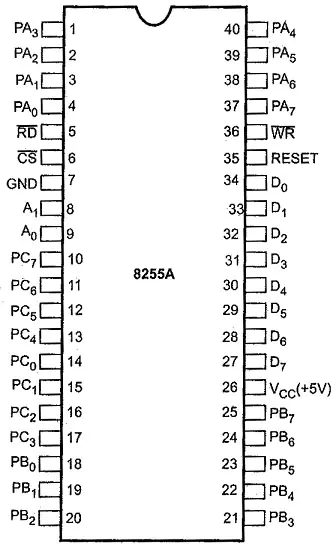
In the 8255 programmable peripheral interface, the 8255 microprocessor’s pin diagram is displayed below. 40 pins, including PA7-PA0, PC7-PC0, PC3-PC0, PB0-PB7, RD, WR, CS, A1 & A0, D0-D7, and RESET, are included in this microprocessor. We talk about these pins below.
- Pins of port A (PA0 – PA7): The Port A data lines pins 1 to 4 and 37 to 40, which are evenly spaced on both sides of the microprocessor’s top, are PA7 to PA0. These eight port A pins operate as either latched output or buffered input lines, depending on the control word stored into the control word register.
- Pins of port B (PB0 – PB7): The data line pins from 18 to 25 that carry the port B data are PB0 to PB7.
- Pins of port C (PC0 – PC7): Pins 10 through 17 carry the port A data bits, while pins PC0 through PC7 are port C pins. The term “upper pins” refers to pins 10 through 13 and “lower pins” to pins 14 through 17. Four data bits can be transmitted utilising two distinct port C pieces and the pins from these two sections.
- Data pins for the transfer of data (D0 – D7): These D0 to D7 pins, which encompass 27-pin to 34-pin, are data I/O lines. The entire IC work is trained using the 8-bit binary information that is carried by these pins. The control word’s data is carried via these pins, which are collectively referred to as the control register and control word.
- Reset input – RESET: When in set mode, pin35, like the RESET pin, resets all of the data in all of the keys to their initial values. It is an active high signal in which the ports are in the input mode and the control registers are cleared by the high signal at the RESET pin.
- Read input – RD’: The pin that places the chip in the reading mode is pin 5, which is a read input pin like RD’. Through a data buffer, the CPU receives data from a low signal at this RD’s pin.
- Write input – WR’: A write input pin that switches the chip into writing mode is pin36, often known as the WR pin. The microprocessor would otherwise depend on the data bus buffer for control; in other words, a low signal at the WR pin just allows the CPU to carry out the write operation above the ports.
- Chip select – CS’: A chip select input pin, pin 6 like CS’, is in charge of choosing a chip. An active low signal at the CS pin allows data transfer, but a low signal at this pin only allows communication between the 8255 and the CPU.
- Address pins – A1 and A0:Simply select the preferred port for data transmission using the A0 and A1 pins at pins 8 and 9.
- Port-A is chosen if both A0 and A1 are equal to zero.
- Port-B is chosen in the event that A0 = 0 and A1 = 1.
- Port-C is chosen in the event that A0 = 1 and A1 = 0.
- The control register is chosen if A0 and A1 are both equal to 1.
8255 programmable peripheral interface – Features
In the 8255 programmable peripheral interface, The following are some of the characteristics of the 8255 microprocessor.
- A PPI (programmable peripheral interface) device is the 8255 microprocessor.
- It has three I/O ports that can be programmed in various ways.
- This microprocessor only provides many connecting choices for different devices. It is therefore extensively utilised in numerous applications.
- Mode 0 (Simple I/O), Mode 1 (Strobed I/O), and Mode 2 (Strobed bi-directional I/O) are its three operating modes.
- It is completely compatible with the Intel microprocessor family.
- It is compatible with TTL.
- This microprocessor has direct bit SET/RESET capabilities for port-C.
- There are twenty-four programmable input/output pins, which are grouped into two to eight-bit and two to four-bit ports.
- Ports A, B, and C are the three 8-bit ports that are included.
- A control register that specifies the purpose of each I/O port and the mode in which it must function is included with the three I/O ports.
8255 programmable peripheral interface – Advantages
In the 8255 programmable peripheral interface, the following are some of the benefits of the 8255 microprocessor.
- The 8255 microprocessor is compatible with almost all microprocessors.
- It is possible to designate various ports as I/O functions.
- It uses a regulated power supply of +5V to function.
- This coprocessor is widely used.
- The 8255 coprocessor acts as an interface between the CPU and peripheral devices to enable simultaneous data transfers.

